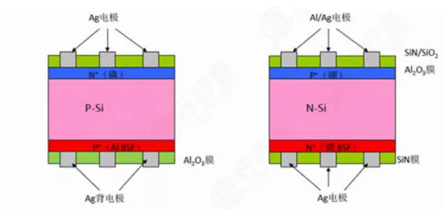
The main differences between N-type and P-type monocrystalline silicon wafers for solar photovoltaic

The main differences between N-type and P-type monocrystalline silicon wafers for solar photovoltaics
Monocrystalline silicon wafers have the physical properties of quasi-metals, with weak conductivity, and their conductivity increases with increasing temperature. They also have significant semiconducting properties. By doping ultra-pure monocrystalline silicon wafers with small amounts of boron, the conductivity can be increased to form a P-type silicon semiconductor. Similarly, doping with small amounts of phosphorus or arsenic can also increase conductivity, forming an N-type silicon semiconductor. So, what are the differences between P-type and N-type silicon wafers?
The main differences between P-type and N-type monocrystalline silicon wafers are as follows:
Dopant: In monocrystalline silicon, doping with phosphorus makes it N-type, and doping with boron makes it P-type.
Conductivity: N-type is electron-conducting, and P-type is hole-conducting.
Performance: The more phosphorus is doped into N-type, the more free electrons there are, the stronger the conductivity, and the lower the resistivity. The more boron is doped into P-type, the more holes are generated by replacing silicon, the stronger the conductivity, and the lower the resistivity.
Currently, P-type silicon wafers are the mainstream products in the photovoltaic industry. P-type silicon wafers are simple to manufacture and have low costs. N-type silicon wafers typically have longer minority carrier lifetimes, and the efficiency of solar cells can be made higher, but the process is more complicated. N-type silicon wafers are doped with phosphorus, which has poor solubility with silicon. During rod drawing, phosphorus is not evenly distributed. P-type silicon wafers are doped with boron, which has a similar segregation coefficient to silicon, and the uniformity of dispersion is easy to control.
