In-Depth Analysis of Photovoltaic Solar Cells: A Comprehensive Guide Part 1
Detailed Analysis of Photovoltaic Solar Cells
Part 1: Photovoltaic Cell Technology Pathways
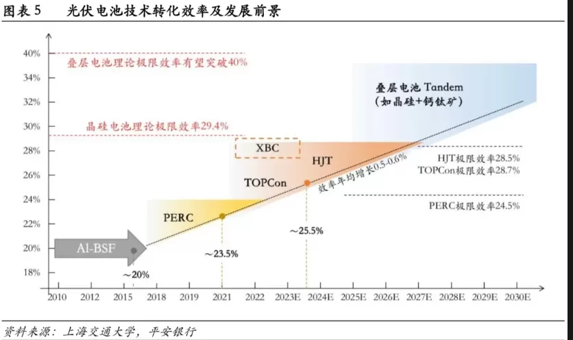
In the solar energy industry, improving efficiency while reducing costs remains the pivotal driving force and a perpetual topic of discussion. Within the extensive solar value chain, the solar cell stands as the core of technological advancement, determining the efficiency limits of photovoltaic (PV) products. Historically, the monocrystalline PERC (Passivated Emitter and Rear Contact) pathway served as a significant turning point, contributing immensely to achieving grid parity for solar power generation. However, as its mass production performance approaches its limits (with conversion efficiency reaching around 23.3-23.5% and non-silicon costs around 0.15 yuan/W), the industry urgently requires the development of novel solar cell pathways with greater upgrade potential.
Since 2022, N-type cell technologies such as TOPCon (Tunnel Oxide Passivated Contact), HJT (Heterojunction with Intrinsic Thin Film), and XBC (eXtended Back Contact) have initiated a new wave of expansion cycles, reshaping the industry landscape. This chapter begins with the working principles of photovoltaic cells, retracing the technological evolution and the differences in cell technologies, thus clarifying the pathways and strategies for enhancing photovoltaic cell efficiency. This lays the groundwork for subsequent analyses of production costs and future trends.
(1) Overview of Photovoltaic Cell Technologies
The working principle of photovoltaic cells is based on the photovoltaic effect, first discovered by French scientist Edmont Becquerel in 1839. Under illumination, photons with energy greater than the semiconductor bandgap are absorbed by the semiconductor, exciting electrons from the valence band to the conduction band, thus creating electron-hole pairs. In a structure composed of P-type and N-type semiconductors, the built-in electric field directs the movement of electrons and holes, generating electric current.
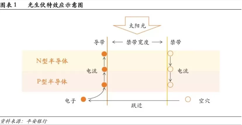
The semiconductor material's bandgap width significantly impacts the solar cell's short-circuit current and open-circuit voltage (short-circuit current increases with a decrease in bandgap width, while open-circuit voltage decreases). Consequently, it is theorized that suitable semiconductor materials for photovoltaic cells should have a bandgap width between 1.1-1.6 eV. This framework has given rise to three generations of solar cell technology routes: crystalline silicon solar cells, inorganic thin-film solar cells, and new solar cells represented by perovskite materials. Currently, the global photovoltaic market is dominated by the more mature crystalline silicon cells, which, according to CPIA statistics, accounted for approximately 96.2% of the market share in 2021.
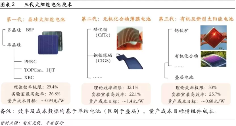
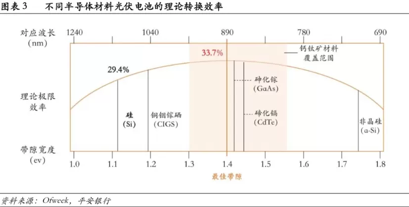
Crystalline silicon has a bandgap width of 1.12 eV, allowing it to absorb about 49% of photon energy at room temperature while effectively outputting around 60% of electric energy due to the differences in the bandgap potential and open-circuit voltage. Therefore, the efficiency limit of silicon-based single-junction solar cells at room temperature is approximately 29.4%.
Theoretically, the optimal bandgap width for semiconductors is around 1.4 eV, which could enable a theoretical efficiency limit of 33.7%. Perovskite materials fall within this optimal bandgap range, while cadmium telluride and other thin-film materials also closely approach the ideal bandgap width. As a result, the second and third generation of cell technologies possess higher theoretical efficiency limits compared to the first generation of crystalline silicon cells. Moreover, stacking different semiconductor materials to create multi-junction solar cells can further expand photon energy absorption, potentially elevating efficiency limits beyond 40%. This represents a crucial future development direction for photovoltaic cell technology.
This report primarily focuses on the current mainstream crystalline silicon cell technology.
Despite the theoretical efficiency limit of crystalline silicon cells being only 29.4%, real-world energy losses mean that the highest experimental efficiency currently achieved is about 26.8%, with mass production efficiency at approximately 26%. This indicates that there is still room for improvement.
Specifically, energy losses can be classified into optical losses and electrical losses. Optical losses occur when photon energy is not absorbed by the silicon substrate, resulting from factors like surface reflection, long-wave projection, or electrode gridline shading. Electrical losses can be further divided into recombination losses and ohmic losses (resistive losses). The former refers to the reduction in current due to electron and hole recombination before generating current, while the latter refers to losses occurring during current transmission due to resistance. The core of photovoltaic cell technology development lies in optimizing cell structures and materials to minimize both optical and electrical losses.
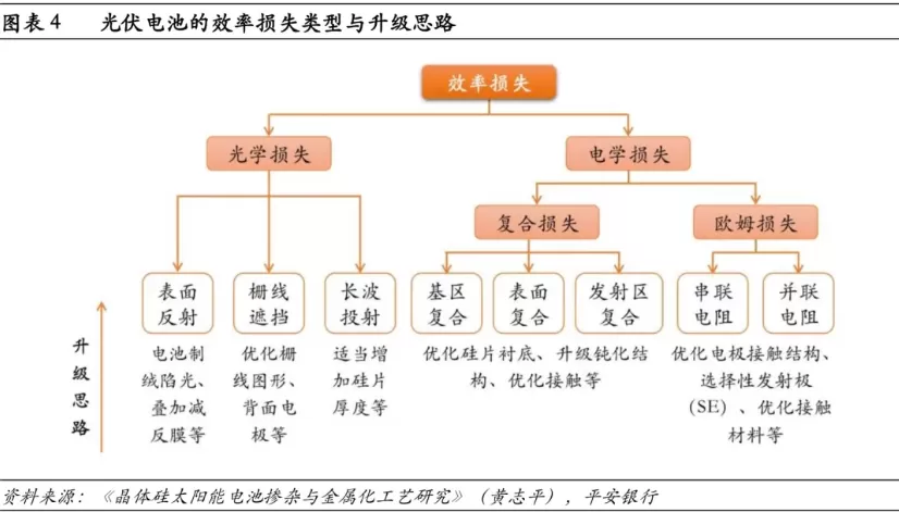
From the earliest commercially successful aluminum back surface field (Al-BSF) cells to the PERC cells that facilitated grid parity for solar energy, the efficiency enhancement strategy primarily focused on optimizing passivation structures and electrode contact methods to reduce recombination and ohmic losses. With the advent of the N-type cell era, both TOPCon and HJT cells adopted "passivated contact" technology to further diminish electrical recombination losses. Meanwhile, the BC (Back Contact) cell took a different approach by relocating the front surface electrodes to the back, thereby reducing gridline shading and consequently minimizing optical losses. As a versatile technology, it can also synergistically combine the advantages of TOPCon and HJT cells, giving rise to the more efficient XBC cell pathway. Looking ahead, breakthroughs in the research of new materials like perovskite hold promise for advancing a new generation of solar cells and allowing crystalline silicon cells to merge with new materials, exploring breakthroughs toward higher efficiency limits in multi-junction cells.
(2) Photovoltaic Cell Structure and Efficiency Enhancement Strategies
From BSF to Monocrystalline PERC
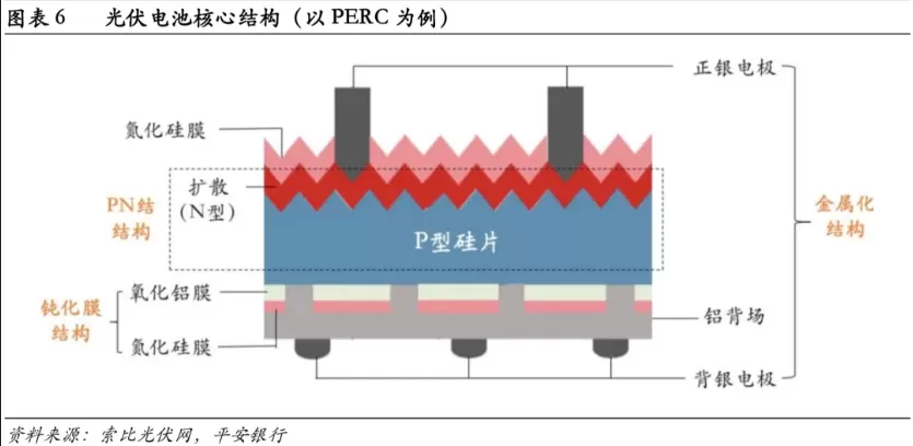
The primary structure of crystalline silicon cells includes the PN junction, passivation films, and metallization electrodes. The PN junction serves as the heart of photovoltaic cells, formed by a negatively charged P-type region and a positively charged N-type region. The built-in electric field they create directs the movement of electrons and holes, generating current. The passivation film reduces surface recombination losses, while the metal electrode gridlines collect current and conduct it externally.
Taking PERC cells as an example, phosphorus doping on a P-type silicon substrate forms the N-type emitter region, which, together with the silicon wafer, constitutes the PN junction. An aluminum oxide layer and a silicon nitride film are deposited on the cell's back surface to provide passivation and reduce reflection. The front surface's positive silver electrode and the aluminum back surface, along with the back silver electrode, form the cell's metallization structure. Additionally, the “inverted pyramid” light-trapping structure on the front surface, along with the silicon nitride film, aims to minimize surface reflection.
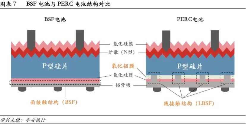
Before the advent of PERC cells, aluminum back surface field cells (Al-BSF) were the first crystalline silicon cell structure to achieve commercialization, first proposed in 1973 and exceeding 90% market share by 2016. While BSF cells have the advantages of a simple process, low cost, and mature technology, the full-area contact between the aluminum back surface and silicon substrate leads to significant surface recombination losses, preventing cell efficiency from exceeding the 20% threshold.
PERC, proposed in 1989 by a research team led by Martin Green at the University of New South Wales in Australia, utilized silicon oxide as the passivation membrane and anti-reflective layer initially, which made the technology complex and costly. It wasn't until around 2010, when aluminum oxide (Al2O3) was adopted as the passivation interface layer, that PERC cells began their journey towards industrialization. Compared to BSF cells, PERC's improvements mainly focus on two aspects: the addition of a back aluminum oxide layer for passivation and a shift from surface contact to line contact with the aluminum back surface.
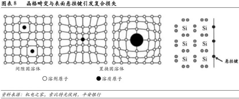
The passivation mechanism involves both field-effect passivation and chemical passivation. The former generates an electric field at the interface that repels similarly charged carriers, thus reducing recombination, while the latter saturates dangling bonds at crystal defects in silicon with free hydrogen, enhancing chemical passivation.
Aluminum oxide serves as an optimal passivation material for P-type silicon surfaces. It carries a negative charge, allowing for efficient field passivation effects at the interface between aluminum oxide and the silicon crystal surface. Furthermore, the deposition process of aluminum oxide provides sufficient hydrogen atoms to saturate the dangling bonds on the silicon surface, thus effectively enhancing chemical passivation. After implementing the aluminum oxide film as a passivation layer, PERC cell efficiencies surpassed those of BSF cells by over 1%.
In terms of contact methodology, the contact between the metal electrode and silicon substrate leads to substantial minority carrier recombination at the contact interface, adversely affecting conversion efficiency. PERC cells transitioned from full-area contact with the aluminum back surface to line contact, thereby minimizing contact area and reducing recombination losses.
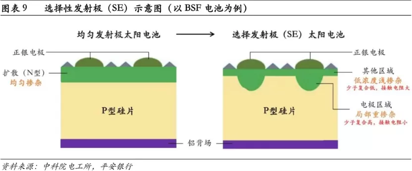
Additionally, PERC cells adopted the selective emitter (SE) technology on the front surface to decrease resistance and recombination losses. This technique involves creating a high-concentration phosphorus doping region at the contact points between the metal electrode and the N-type region of the PN junction, establishing a gradient of impurity concentrations to enhance carrier collection and reduce resistance. However, high-concentration doping can also increase surface recombination losses; therefore, selective high-concentration doping is implemented locally to balance resistance losses and recombination losses effectively. The industry gradually incorporated SE technology around 2017, driving PERC cell conversion efficiencies to approximately 23.5%.
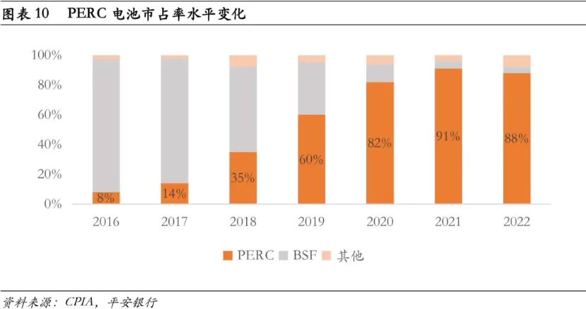
As PERC cell technology has matured and production processes have advanced, PERC cell market share has been increasing at an annual rate of roughly 20% since 2017, overtaking BSF cells in 2019 to achieve a market share of around 91% by 2021.
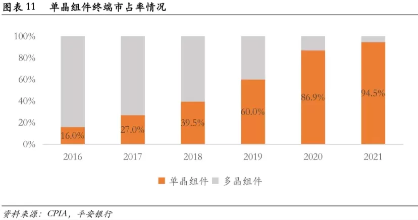
During the same period, photovoltaic cells also underwent a competition between monocrystalline and polycrystalline silicon wafer materials. Monocrystalline silicon wafers exhibit superior lattice arrangement with fewer internal defects and impurities, leading to better electrical performance and conversion efficiency compared to polycrystalline wafers. Following the industry’s resolution of issues like cell thermal mismatch (CTM) and light-induced degradation (LID) for monocrystalline components starting in the latter half of 2015, the market penetration of monocrystalline cells began to rise steadily. By 2019, monocrystalline module market share exceeded 50%, reaching 60% in 2020 and further increasing to 86.9%, effectively becoming the market mainstream, while polycrystalline components began to exit the market entirely by 2021.
From P-Type Silicon Wafers to N-Type Silicon Wafers
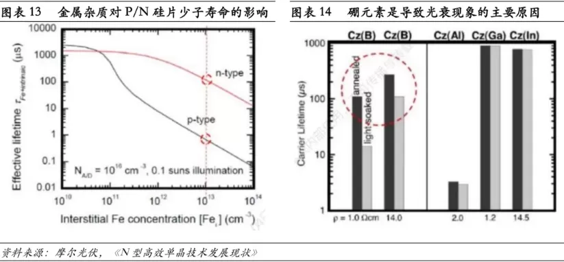
Doping impurities in silicon wafers can produce either P-type or N-type wafers, with the primary difference being the type of dopant used. P-type wafers are primarily doped with boron or gallium, with electrons as minority carriers; N-type wafers are doped with phosphorus, with holes as minority carriers. N-type wafers demonstrate numerous advantages over P-type wafers, including longer minority carrier lifetimes, higher impurity tolerance, lack of light-induced degradation, and lower temperature coefficients.
The performance discrepancies between P-type and N-type wafers stem primarily from the stronger positive charge of metal impurities like Fe, Cu, and Ni, which have a greater tendency to capture electrons. Thus, N-type wafers, with holes as minority carriers, tend to exhibit much longer minority carrier lifetimes compared to P-type wafers under the same metal impurity conditions (research indicates that N-type wafers with equal resistivity can achieve minority carrier lifetimes 1-2 orders of magnitude longer than their P-type counterparts). Higher minority carrier lifetimes correlate with improved photovoltaic conversion efficiency, making N-type wafers more efficient.
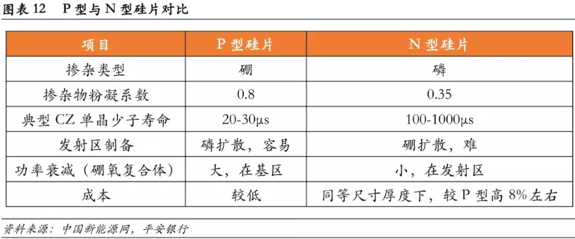
In addition, boron in P-type wafers can form boron-oxygen complexes under light exposure or current injection, which capture carriers and reduce minority carrier lifetimes, leading to light-induced degradation (LID). The current industry approach to mitigate light-induced degradation in P-type wafers involves lowering boron or oxygen content, typically through high-purity crucibles for monocrystalline growth or co-doping with gallium to reduce boron levels. However, the former can inflate costs, while the latter may degrade cell efficiency. Conversely, N-type wafers, with minimal boron content, naturally reduce the occurrence of light-induced degradation.
Previously, N-type wafers faced limitations due to immature processing technology and high costs. However, with the continued development of N-type wafer-based cell technologies like TOPCon and HJT and ongoing advancements in wafer processing techniques, N-type wafers are expected to gain market share and gradually replace P-type wafers.
N-Type Cell Technologies: TOPCon and HJT
(1) TOPCon Cells
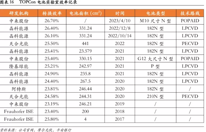
TOPCon, short for Tunnel Oxide Passivated Contact, was first proposed by the Fraunhofer Institute at the 28th European PVSEC conference in 2013. They achieved a laboratory efficiency record of 25.8% on 4cm² cells by 2017. According to theoretical models established by Jan Schmidt and others in 2018, the theoretical efficiency limit of TOPCon cells is estimated to be 28.7%.
The distinctive feature of TOPCon cells is the use of a tunneling oxide layer combined with doped polycrystalline silicon for passivated contact technology. This means that a thin dielectric film isolates the metal electrode from the semiconductor, allowing for carrier tunneling while passivating the silicon surface, effectively reducing recombination losses incurred from direct metal contact. In the TOPCon cell structure, the silicon oxide layer (SiO2) plays a dual role in passivation and tunneling. The doped polycrystalline silicon layer not only forms a high-low junction structure with the N-type silicon substrate, minimizing recombination losses at the silicon interface but also provides excellent carrier conduction properties.
In addition to these features, TOPCon differs from PERC cells in several ways: (1) TOPCon cells use N-type silicon substrates, leading to a different doping structure for the PN junction compared to PERC cells, which use phosphorus doping; (2) due to the low concentration of boron doping, the front surface emitter region experiences higher resistance, necessitating the use of silver-aluminum paste to create metal fine grids that allow aluminum atoms to enter the emitter region during sintering to form a P+ region, thereby reducing resistance; (3) because the back side employs a passivated contact structure, the metal electrodes no longer need to contact the silicon substrate, allowing for the elimination of aluminum back surface fabrication and laser grooving; (4) TOPCon cells retain the passivation and anti-reflective structures (aluminum oxide and silicon nitride) from PERC cells, but they have been relocated to the front surface.
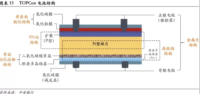
To date, mass-produced TOPCon cells have only adopted the passivated contact structure on the back surface, while the front surface continues to utilize the PERC cell's aluminum oxide and silicon nitride passivation structure, leading to some efficiency losses. To achieve the theoretical efficiency limit of 28.7%, TOPCon cells must complete a bifacial passivated contact structure; however, the theoretical limit for cells with only back-side contact is about 27.1%. The highest laboratory efficiency records among domestic manufacturers for TOPCon cells have been achieved by Zhonglai Technology, which attained a conversion efficiency of 26.7% on M10-sized N-type cells in April 2023, surpassing the previous record of 26.4% set by JinkoSolar on 182 N-type cells in December 2022. Other leading domestic companies that have engaged in TOPCon research include Trina Solar, Canadian Solar, and LONGi Green Energy.
(2) HJT Cells
HJT, or Heterojunction with Intrinsic Thin Film, was initially proposed by Japan's Sanyo Electric in the late 1980s and patented under the HIT trademark in 1991. Following the expiration of the patent in 2011, both domestic and international manufacturers began scaling up their laboratory research and production of heterojunction cells. In 2021, LONGi's Wei Long and colleagues calculated the theoretical efficiency limit for HJT cells to be 28.5%, giving them a competitive edge over single-sided TOPCon cells.
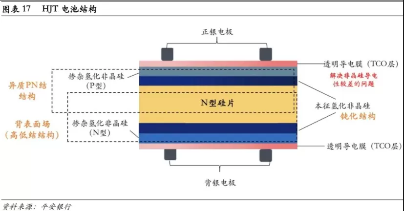
PERC and TOPCon cells create their PN junctions directly on silicon substrates through doping, resulting in homojunction structures. In contrast, HJT cells consist of a PN junction formed by an N-type silicon substrate (c-Si) and doped amorphous silicon thin films (a-Si), thus referred to as heterojunction cells.
Structurally, HJT cells utilize an N-type silicon substrate and first deposit intrinsic hydrogenated amorphous silicon (a-Si:H) thin films on the front and back surfaces for passivation. Subsequently, a P-type doped hydrogenated amorphous silicon layer is deposited on the front surface, which, together with the silicon substrate, forms the PN junction. On the back, an N-type doped hydrogenated amorphous silicon layer is deposited to form the high-low junction (N+/N) structure. Given the high contact resistance of hydrogenated amorphous silicon, a transparent conductive oxide (TCO) layer is required to facilitate carrier movement and reduce reflection (ARC). Lastly, due to the stringent temperature requirements (not exceeding 200°C) for hydrogenated amorphous silicon, HJT cell fabrication is performed using low-temperature processes, with the metal electrode paste adjusted to low-temperature silver paste instead of the high-temperature silver paste used for PERC and TOPCon cells.
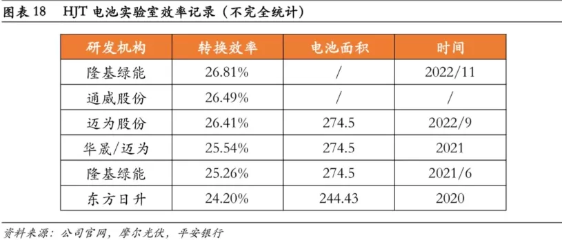
The current highest laboratory efficiency record for HJT cells was achieved by LONGi Green Energy in November 2022, with their microcrystalline technology HJT cell reaching a conversion efficiency of 26.81%, surpassing the previous record of 26.41% set by Miawei Technology and Sundrive in September 2022. Additionally, leading domestic companies such as Tongwei, Canadian Solar, JinkoSolar, and Trina Solar have developed HJT technology capabilities, while companies like Risen Energy, Huasheng New Energy, Aikon Technologies, and Hanergy have heavily invested in HJT cell pathways.
Platform Technologies: XBC Cells
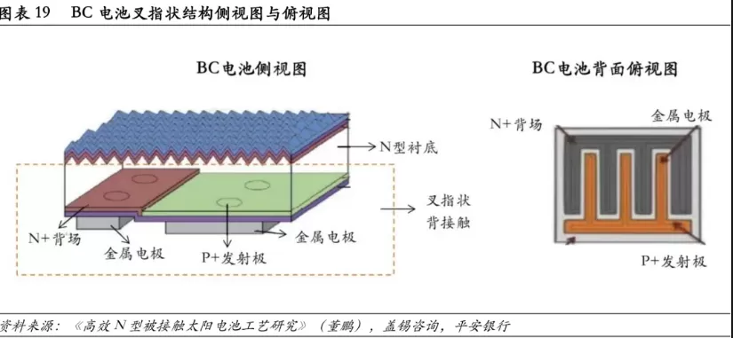
IBC, or Interdigitated Back Contact cells, were first proposed by Schwartz and Lammert in 1975. Their key feature is the arrangement of metal electrodes in a finger-like pattern solely on the back of the cell, along with the corresponding PN junction P-type and high-low N+ regions also arranged in a finger-like pattern on the back. This design aims to eliminate the shading effect caused by the front metal electrode gridlines, thus maximizing incident light utilization and minimizing optical losses. Simultaneously, since there is no shading to consider, the metal gridlines can be made wider, thereby reducing resistance, while the doping concentrations in the PN junction can be minimized to reduce recombination losses. To ensure that photogenerated carriers are not substantially recombined before reaching the back PN junction, IBC cells typically require higher minority carrier lifetimes, achieved by using higher lifetime P-type silicon or directly employing N-type silicon to ensure higher carrier collection rates.
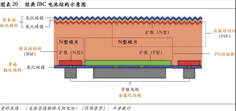
Classic IBC cells utilize N-type silicon wafers as substrates, doping the front surface with phosphorus to form an N+/N front surface field (FSF) to reduce surface recombination losses. The back surface is doped with phosphorus and boron to form interdigitated P+ emitter and N+ back surface field (BSF) regions. The P+ emitter and the silicon substrate together form the PN junction, while the N+ back surface forms the high-low junction with the substrate. Passivation layers of stacked silicon oxide and silicon nitride are utilized on both the front and back surfaces. The width of the P+ emitter and N+ back surface, along with the spacing between them, significantly influences cell performance. Generally, the widths of the N+ back surface and the spacing should be minimized, which increases the difficulty of fabrication processes.
Due to the unique efficiency enhancement strategies adopted by IBC cells, they not only leverage their strengths but also offer compatibility with other cell technologies, being referred to as BC (Back Contact) cells or XBC cells. Theoretically, the BC structure can enhance cell conversion efficiency by 0.6-0.7%, positioning it as a highly promising platform technology likely to become the next mainstream technological route. Specifically:
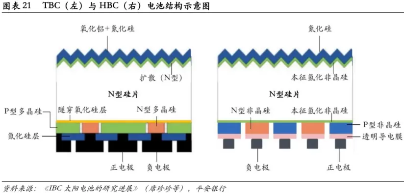
(1) Combining with the TOPCon Route to Form TBC Cells: Using N-type silicon wafers as substrates, the front surface undergoes phosphorus doping to create an N+ front surface field, with aluminum oxide and silicon nitride layers deposited for passivation and anti-reflection. A tunneling oxide layer is applied to the back, alongside interdigitated P-type and N-type doped polycrystalline silicon layers, finished with a silicon nitride passivation layer, with openings made to create positive and negative electrodes.
(2) Combining with the HJT Route to Form HBC Cells: Utilizing N-type silicon wafers, the front surface is deposited with hydrogenated amorphous silicon thin films for passivation, replacing the transparent conductive film with a silicon nitride anti-reflective layer. On the back, hydrogenated amorphous silicon thin films are deposited as passivation layers, alongside interdigitated P-type and N-type doped thin films, concluding with a transparent conductive film and openings made for positive and negative electrodes.
American company Sunpower leads and pioneers IBC cells, with the third-generation IBC cells launched in 2015 achieving production efficiencies of 25%. Sunpower's spin-off, Maxeon, is expected to release a seventh-generation product that combines the passivated contact structure of TOPCon cells, with anticipated production efficiencies exceeding 26%. This marks a 2-3% advantage over the contemporaneous mainstream PERC cells and about 1% higher than the N-type cell technologies like TOPCon and HJT. The highest laboratory efficiency record for BC cells stands at 26.7%, achieved by Japan's Kaneka in 2017 using the HBC route. In the domestic market, LONGi Green Energy and Aiko Technology have also achieved mass production, with LONGi's HPBC products achieving production efficiencies of 25.3%, while Aiko's ABC products boast a production efficiency of 26.5% (specific route details yet to be disclosed).
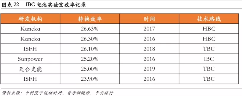
In addition to efficiency advantages, BC cells are aesthetically pleasing due to the absence of gridline shading on the front, and if the cell frame is also modified to black materials, a fully black module product can be produced. However, the back gridline structure does slightly compromise the bifaciality of BC cells, limiting their ability to capture ground-reflected light and increase energy generation.
Conclusion
As the photovoltaic industry evolves, it is evident that the development of advanced solar cell technologies is critical for achieving higher efficiency and lower costs. With innovative pathways like TOPCon, HJT, and XBC cells gaining traction, the future of solar energy looks promising. By focusing on optimizing structures, materials, and processes, we can unlock the potential for even greater advancements in solar power generation.
As a company with 15 years of experience in the solar industry, Ooitech is dedicated to providing state-of-the-art manufacturing equipment for solar panels and modules, including G1, M6, M10, M12, and various advanced technologies. We offer comprehensive training and support for production line setup, ensuring our clients achieve the highest levels of efficiency and output. For more insights, subscribe to our YouTube channel for updates on solar factory innovations and watch our MBB Full Automatic solar panel production line video. Download our catalog and learn more about our company in our company profile. If you have any inquiries, feel free to reach out via email at [email protected] or contact us on WhatsApp at +8615961592660.
