In-Depth Analysis of Photovoltaic Cell Manufacturing Process and Cost Analysis (Part 2)
Detailed Analysis of Photovoltaic Cell Manufacturing Process and Cost Analysis (Part 2)
Introduction
The solar energy industry has seen significant advancements over the past few decades, particularly in the field of photovoltaic (PV) cells. Despite evolving technologies, the fundamental principles and core structures of crystalline silicon cells have remained largely unchanged. This article delves into the intricacies of the PV cell manufacturing process, focusing on core steps such as cleaning, diffusion, deposition, and metallization. Furthermore, it will analyze the cost implications of different technologies including TOPCon, HJT, and XBC.
Core Processes and Technological Differences
1. Cleaning and Texturing
Cleaning and texturing form the first crucial step in PV cell manufacturing. The cleaning process utilizes alkaline solutions to remove oil, metal contamination, and mechanical damage from the silicon wafer's surface, thereby minimizing impurities that may adversely affect yield. Texturing, on the other hand, employs a technique where silicon wafers are etched to create a pyramidal structure that increases the surface area, significantly reducing light reflection losses.
The predominant method for cleaning is wet processing, which involves chemical solutions to dissolve contaminants. Current cleaning equipment includes single wafer and batch cleaning systems. For PERC and TOPCon technologies, the cleaning and texturing stages are similar; however, HJT technology requires different equipment due to its low-temperature processing requirements. Japanese companies dominate the semiconductor cleaning equipment market, but domestic manufacturers like Jiejia Weichuang and Beifang Huachuang are rapidly catching up.
2. Diffusion and Junction Formation
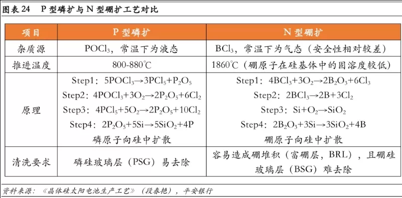
Diffusion and junction formation involve creating the PN junction through high-temperature chemical diffusion. This process introduces dopant elements into either P-type or N-type silicon wafers, subsequently increasing hole or electron concentration and establishing an internal electric field. PERC and TOPCon technologies typically utilize low-pressure tube diffusion furnaces, while HJT cells employ ion implantation and chemical vapor deposition (CVD) methods.
The diffusion equipment for PERC cells has been completely localized in China, while the TOPCon process, which involves boron diffusion, requires higher uniformity and temperature, leading to increased equipment costs. The laser doping technique is also gaining traction for creating selective emitter structures.
3. Deposition and Coating
Deposition is crucial for forming various thin film layers within the cell structure, including aluminum oxide and silicon nitride in PERC cells, and tunneling oxide and doped polysilicon layers in TOPCon cells. The deposition processes can be categorized into physical vapor deposition (PVD), chemical vapor deposition (CVD), and atomic layer deposition (ALD). Each method has its unique characteristics and is chosen based on the specific requirements of the film layers.
For instance, the deposition of aluminum oxide in PERC cells is primarily performed using ALD due to its superior passivation properties. In contrast, TOPCon cells utilize a combination of LPCVD and PECVD for various layers, while HJT cells predominantly rely on PECVD and CAT-CVD.
4. Metallization
Metallization involves applying metal paste to the cell's front and back surfaces to create electrical contacts. TOPCon and HJT technologies have simplified metallization by eliminating the aluminum backfield and requiring only the formation of finger and busbar structures. The choice of metal paste significantly impacts the overall cost and efficiency of the cells. HJT technology often requires low-temperature silver paste, which can be more costly due to the absence of glass powders used in high-temperature processes.

Cost Analysis of Different Cell Technologies
1. TOPCon Technology
TOPCon cells offer a competitive edge due to their compatibility with existing PERC production lines. The initial investment for TOPCon production lines is estimated to be around 1.6 billion CNY/GW for PECVD and slightly higher for LPCVD. These costs are justified by the potential for lower silicon wafer costs due to thinner wafers, which can achieve thicknesses of 130μm or less.
The overall production cost for TOPCon cells is approximately 0.44 CNY/W, with non-silicon costs around 0.20 CNY/W. The major cost contributors include equipment depreciation and the higher cost of electrode paste, which adds approximately 2.4 fen/W compared to PERC technology.
2. HJT Technology
HJT technology simplifies the production process to just four main steps, which can lead to lower defect rates and production costs. However, it requires entirely new production lines, leading to a capital investment of around 3.64 billion CNY/GW. HJT cells typically exhibit lower silicon costs due to their thinner wafers, achieving thicknesses as low as 120μm or even 100μm for leading manufacturers.
The current production cost of HJT cells is about 0.50 CNY/W, with non-silicon costs around 0.27 CNY/W. Efforts to integrate technologies like 0BB (Zero Busbar) with copper-plated silver or copper deposition are anticipated to further reduce costs.
3. XBC Technology
XBC technology, which combines various doping methods and has increased requirements for patterning, generally incurs higher production costs due to additional equipment and process steps. The investment for XBC production lines includes the cost of deposition equipment and laser systems, estimated to increase the overall cost by approximately 800 million CNY per GW.
The production costs for XBC cells are further influenced by the necessity of wider silver paste lines, which effectively double the silver consumption compared to PERC cells. Innovations such as the 'no-silver' technology developed by Aiko and others aim to mitigate these costs while enhancing efficiency.
Conclusion
As solar technology continues to evolve, understanding the manufacturing processes and cost structures of different photovoltaic cells is crucial for stakeholders in the industry. Technologies such as TOPCon and HJT present unique advantages and challenges, influencing overall production costs and efficiency. Companies like Ooitech, with over 15 years of experience in the solar industry, provide a range of manufacturing equipment and process training for solar panel production lines. For more information and resources, you can visit our YouTube channel or download our catalog.
